S2DI Engineering Consulting
Precision Electronics Design & Integration
Providing end-to-end design services for projects requiring application specific PCB design or system integration. Expertise in full-stack hardware development including: SPICE simulation, PCB layout, firmware development, and system integration.
THERMAL / MECHANICAL RELIABILITY
RF & High-Speed Digital
Strict Physical Constraints
DFM-Optimized Layouts
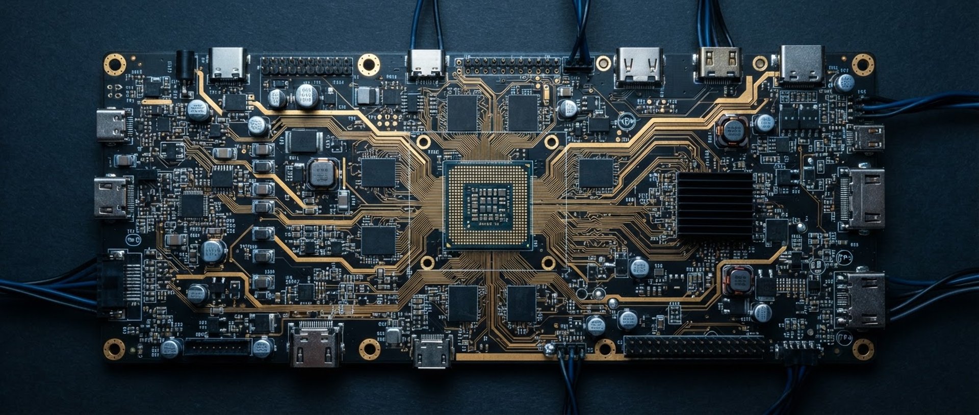
Deliberate trace routing and impedance matching to eliminate EMI issues and ensure clean signal propagation across multi-layer boards.
Advanced copper pour strategies and via-in-pad structures designed to manage heat dissipation in high-density environments.
Rigorous design-for-manufacturing rules applied directly to the layout, ensuring seamless fabrication and assembly at scale.
Our Design Methodology
Define Customer Needs
Iterative Design Approach
In-Person System Integration
We will work with your team to determine what your needs are and how we can best assist. A project requirements document will be created before any work begins.
With regular status updates, iterate on individual components within the full system to ensure meeting customer requirements.
An expert from our team will be available to assist in any installation / integration of a design into an existing system. We are flexible and willing to meet any of our customer needs.
Collaborate
Send us your idea. Regardless of the stage in product development cycle, our time will identify and assist you with delivering your project to the finish line.
S2DI
Precision PCB Layout & Hardware Integration
SITEMAP
Home
Capabilities
About
Contact
GET IN TOUCH
sam@s2-di.com
Response within 1 business day
© 2026 S2DI - Selyutin Systems & Design Integration - CONSULTING
ACHIEVING EXCELLENCE THROUGH COMMUNICATION